
PCB Design USB Oscilloscope
An analog input USB oscilloscope PCB was designed to filter out high-frequency input signals, scale and shift signals, as well as remove DC offset during AC coupling.
B A C K G R O U N D
Figure 1 below depicts the circuit diagram for a do-it-yourself oscilloscope whose output is sent to an Arduino. The circuit involves three primary stages of circuitry: (1) a summing operational amplifier, (2) a capacitor, and (3) an inverting op-amp. The first op-amp accepts the input signal from a probe, which is then scaled with a gain of 1 or 0.5, depending on the configuration of the switch. A second switch then enables or prevents access to a single capacitor that is used for coupling: AC when the switch is open and DC when the switch is closed. Finally, the inverting op-amp at the end of the circuit reverses the negative gain of the first op-amp, thus returning the signal to the same sign as the input.
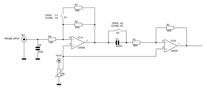
Fig. 1: Circuit Diagram for DIY Arduino Oscilloscope [1]
An issue with this design is the pole at the origin (s=0) caused by the lone coupling capacitor. As a result, it is necessary to adjust the final implementation of the coupling capacitor such that the pole it creates is cancelled out.

Fig. 2: Circuit Diagram for Sound Card Oscilloscope [2]
Figure 2 above depicts the circuit diagram of a simple sound card oscilloscope. This circuit provides four major functions (as labeled): (1) AC Coupling, (2) Input Protection, (3) 1x/10x Amplifier, and (4) Output Trimmer. Firstly, as with the DIY oscilloscope sample circuit in Figure 1, Figure 2 demonstrates the use of an AC coupling capacitor in order to remove DC offset from the incoming signal. However, any input to this circuit must pass through the coupling capacitor, which is not desired for our objective, since an option between AC coupling and DC coupling is preferred. In this case, a switch is necessary. This stage of the circuit also shows how to achieve a 1M impedance looking into the input voltage terminal, by adding a 1MΩ resistor.
The 1x/10x amplifier of this circuit makes use of an efficient method to alternate between different amplifications. This strategy is to connect a switch to one resistor that prevents or enables access to it by the rest of the circuit, based on the desired gain of the output. For our project, this can be implemented to scale each probe (1x and 10x) appropriately, such that they produce the same output range (0V-5V).
O B J E C T I V E
The objective of this project is to develop a design for the analog input of a USB oscilloscope. Specifically, this oscilloscope should be capable of filtering out high-frequency input signals, scaling and shifting signals to an appropriate range, as well as removing DC offset during AC coupling.
The PCB should
-
Take an input voltage of -15V to +15V (1x Probe) or -1.5V to +1.5V (10x Probe), and scale and shift to an output voltage signal of 0V to +5V using summing op-amps
-
Have a switch for AC/DC Coupling
-
AC Coupling: Block DC component of input signal using a coupling capacitor and attenuate frequencies greater than 20 kHz using a low pass filter
-
DC Coupling: Pass the input signal unchanged
-
-
Prevent attenuation of low frequency input signals during AC Coupling Mode (i.e: Prevent bandpass filter behaviour by canceling out coupling capacitor pole)
R E S U L T S
Candidate Design 1:

Fig. 3: Candidate Design 1 with 7 Op-Amps
This design is based off of a set of seven operational amplifiers, for which an input signal passes through a maximum of five op-amps and a minimum of two. Starting from the left side of the schematic, the very first op-amp features a capacitor which removes the DC offset of any AC signal. This circuit is improved however by using an op-amp with a transfer function equal to -1 with no effective zeros or poles, thus preventing unwanted filtering. This is accomplished by having one zero and one pole that are equal and cancel each other out. The next two op-amps accomplish low-pass filtering.
Selecting the correct resistor and capacitor values, the corresponding gain shall be 1, and the pole shall be equal to 20 kHz or 125.664 krad/s. In the case of a DC signal (where AC coupling and low pass filtering are not needed), a switch encompassing the first three op-amps can be closed, thus short-circuiting and skipping over these components.
The final four op-amps of this circuit are actually a choice between one of two paths of two op-amps, both of which scale and shift the incoming voltage signal to the desired 0 to +5 V. Namely, the signal is scaled using an inverting op-amp, which is subsequently sent to a summing op-amp along with an additional scaled DC input.
Candidate Design 2:

Fig. 4: Candidate Design 2 with Inverting Amplifier, Buffer, Voltage Divider and Summing Amplifier
The second candidate design uses an inverting amplifier, a buffer with a voltage divider, and a summing amplifier to shift and scale the incoming signal. The single pole, double throw switch above R5 creates a short circuit; this means that with a 1x probe, the current will not go through R5 but with a 10x probe the current will go through both R4 and R5. Since both AC coupling and DC coupling need to be scaled to have a gain between 0V and +5V, another switch can be used. When open, the AC input signal will go through a capacitor to remove the DC offset and then through a low pass filter. After the filter it will be scaled and shifted similar to the way the DC signal was. Although the capacitor simplifies the task of reducing the DC offset in the beginning, it also attenuates the lower frequencies and acts as a high pass filter — this is not ideal for the purpose of the design.
Final Design:


Fig. 5: Final Candidate Design Stage 1 (top, left), Stage 2 (top, right), Stage 3 (bottom, left), Stage 4 (bottom, right)
The proposed solution is one that combines the AC attenuating low-pass filter design from Candidate 1 and the shifting and scaling operational amplifier design from Candidate 2. By using the first design’s AC coupling circuit the problem of unwanted filtering from the single capacitor in Candidate 2 can be resolved. Furthermore, by combining the second candidate’s shifting and scaling design, the number of op-amps required is decreased and results in a single output pathway.
Stage 1 consists of 10µF capacitor, with an AC/DC switch, 1 MΩ grounded resistor, and a single stage low pass filter with a buffer to implement gain of 1. Stage 2 contains a summing amplifier combining the inverting amplifier and buffer in order to achieve a output voltage signal of 0V or +5V depending on the 1X or 10X probe switch. Stage 3 consists of the Arduino Nano, SX1308 module, and the +15V input power supply. Stage 4 contains the -15V input power supply with the MC34063AP regulator for DC-DC conversion.


Fig. 6: EAGLE PCB Design Schematic (left) and PCB with Soldered Components (right)
Based on the arrangement of the circuit schematic, Eagle was used to generate the following traces for use on a Printed Circuit Board (Fig. 6). Validating the design, several tests and observations were noted:

Troubleshooting towards the desired results include building the circuit onto a breadboard and testing the voltages through the circuit at each of the various Op-Amp stages.
C O N C L U S I O N
Although soldering the components onto the PCB did not result in a complete functional oscilloscope device, several key aspects of the oscilloscope were observed based on workbench oscilloscope measurements of individual stages of the circuit. By testing individual stages, the
root-cause of the problem was identified as an interference between soldered pins due to the solder not adhering to the copper film on the PCB. The noise seen in the output may also have been due to the soldering job as individual components when tested on a manufactured oscilloscope works well.
For future implementation, it may be beneficial to prepare multiple PCBs as it is both more economical when ordering in larger quantities but also more forgiving to soldering errors.

Fig. 7: Arduino Oscilloscope Output
R E F E R E N C E S
-
P. Ranjan, "A PC and an Arduino: here’s your DIY Oscilloscope", Open Electronics, 2014. [Online]. Available: https://www.open-electronics.org/guest_projects/a-pc-and-an-arduino-heres-your-diy-oscilloscope/. [Accessed: 12- Feb- 2019].
-
P. Horowitz and W. Hill, The Art of Electronics, 2nd ed. Cambridge University Press, 1989.